Project Description
From REuP Project
| Revision as of 07:26, 15 July 2010 Apiotro (Talk | contribs) (→Software to hardware conversion) ← Previous diff |
Revision as of 07:26, 15 July 2010 Apiotro (Talk | contribs) (→Reconfiguration) Next diff → |
||
| Line 62: | Line 62: | ||
| ==Reconfiguration== | ==Reconfiguration== | ||
| + | |||
| + | As mentioned above, the proposed processor cannot be efficiently implemented in commercially available reconfigurable devices. Dedicated ASIC is required. It should support high reconfiguration data transfer, with the possibility of free access to any part of the die. Reconfiguration restricted to just a row or column of existing resources, as it can be done in off-the-shelf FPGAs, increases the configuration data transfer and wastes the resources needlessly. | ||
Revision as of 07:26, 15 July 2010
Contents |
Instructionless processor architecture using dynamically reconfigurable logic
Abstract
In this project we would like to propose the idea of the general-purpose processor implemented in dynamically reconfigurable FPGA. The novelty of the presented solution lays in the lack of typical sequential processing – all operations are realized in parallel in the hardware. At the same time the new architecture does not impose any modification of the software development process.
Introduction
For many years the applications of FPGA devices have not been limited only to prototyping or to small volume production. Since the dynamic reconfiguration techniques of FPGAs are commercially available, there are different concepts of using them for acceleration of many types of computations. Initially, the FPGAs were used as coprocessors supporting conventional sequential processors in the most demanding calculations, where the parallel data processing inside the FPGA was very helpful. Since advanced FPGAs are equipped with processor cores, the sequential processing and parallel coprocessing can be implemented in a single die, significantly alleviating the interconnection problems between these two modules. In [1] a slightly modified UNIX OS running on PowerPC of Virtex allows programmers to treat the tasks implemented in the reconfigurable hardware in the same way as software tasks running on PowerPC. Nevertheless, developing a new or porting an existing application to use such a powerful architecture efficiently requires a quite low-level programming approach, which is far from current standards and trends.
Currently an active research is performed in the domain of Application-Specific-Instruction set-Processors (ASIPs), in which the pipeline structure can be customized and utilized in the program through custom instructions. An extension to this approach is the No-Instruction-Set-Computer (NISC). The NISC compiler maps the application directly to the datapath [2]. It can achieve better parallelism and resource utilization than conventional instruction-set based compilers. Using this approach up to 70% speedup compared to an instruction-set based compiler has been achieved. The pipeline structure remains constant throughout the entire execution of the program.
In this paper a completely novel solution is proposed. It exploits the parallelism of data processing and resources reuse of dynamically reconfigurable FPGAs, without any impact on development of new applications as well as migration (porting) of the existing ones. The proposed solution is an FPGA-based implementation of general-purpose processor, in which there are no sequentially executed instructions but all tasks are implemented in the reconfigurable hardware, in the completely automatic way. The whole array of configurable blocks can be modified at runtime, except for small part responsible for reconfiguration management. The next chapter presents a main idea of fully reconfigurable general-purpose processor. Then some technical issues such as partitioning, software to hardware conversion and reconfiguration are discussed in more detail. Before the conclusions, some considerations dealing with adaptation of the operating system to the proposed processor architecture are included.
General concept
Bearing in mind that the processor proposed in this paper is intended to be a general-purpose one, it should be able to execute any user application. Since this processor is a kind of fully reconfigurable FPGA, without any typical hard- nor even soft- processor core, the application to be executed should be stored in a memory as a set of bitstreams, which can implement its required functionality when loaded into FPGA in a correct sequence. The same must apply to the operating system, shared libraries, interrupt handlers, drivers, etc. Each bitstream must be loaded into FPGA on demand, when operations corresponding to this bitstream should be performed now or in the near future. This issue is explained in more detail in the next chapter. For general considerations it is enough to assume, that when the operations being performed by a given part of FPGA are finished, this part can be configured with a different bitstream, serving a new functionality. This means that the FPGA should be partially reconfigurable and should support very efficient reconfiguration techniques, which is discussed later.
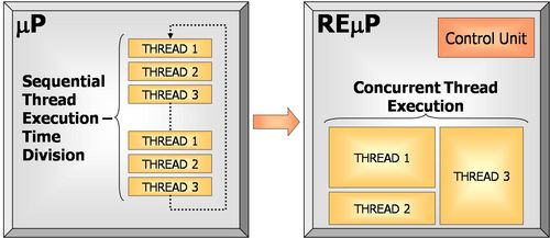
Devoting a part of FPGA for each thread allows running many threads concurrently (Figure 1), without time-division technique. This is a first source of data processing acceleration obtained in the proposed architecture. Obviously, similar acceleration is obtained in multi-core, traditional processors, but this approach is much more flexible and scaleable.
To manage the thread executions (in other words: to load the required bitstreams into the proper FPGA partitions) a special Control Unit is required. This block is the only static module in the FPGA – its configuration cannot be modified at runtime. It must be stressed, that this block does not need to perform any kind of scheduling. The required dependencies between bitstreams should be determined during the bitstream set generation process and stored, together with these bitstreams, in memory. The control block can only suspend a thread execution if there is no place for loading of the new bitstream.
Thread partitioning
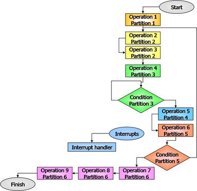
It is obvious, that the functionality of most threads is too complex to be implemented outright in the FPGA at the same time. Therefore it must be split into the sequence of smaller pieces – partitions. The partitions can be in turn composed of several sub-units – operations, optionally finished with a jump (Figure 2).
The exact definition of the operation constitutes still an open issue and must be elaborated by means of some experiments. Currently, it seems that the operation can correspond to a basic block – a part of a program without any jumps out neither in, but probably, some basic blocks should be merged in one operation (e.g. for better loops optimization). To some extent the number of operations in the partition can be adjusted in order to obtain a required partition size.
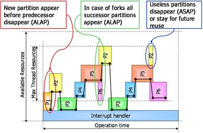
The implementation of the partitions in FPGA should fulfill the following condition: before a given partition is finished, subsequent partition should be implemented (Figure 3). If a given partition is finishing its execution with a jump to one of two subsequent partitions, both partitions should be speculatively prepared for further execution. The implementation of subsequent partitions should take place as late as possible (ALAP).
If the partition is not active any longer, there are two possible solutions. This partition can be marked as stale (as soon as possible – ASAP) in order to release the occupied resources or it can remain implemented for later reuse. The second solution reduces the reconfiguration data transfer but on the other hand it makes the reconfiguration control process and the inter-partition data transfer more complex.
In order to obtain the satisfying flexibility, it should be possible to place the partitions in any part of the FPGA. It means that the current, commercially available reconfiguration techniques, provided e.g. by Xilinx, cannot be efficiently used for this purpose. These techniques require the dynamic partition to be placed in a predefined area, surrounded with special communication blocks (Bus Macros) providing a predefined IO interface.
Another constraint regarding the partitions is that each branching partition must inform the configuration control module about the chosen branch. This can be obtained by setting a dedicated flag implemented inside the partition and reading it by the configuration control unit.
Software to hardware conversion
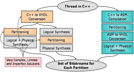
The crucial point of the proposed general-purpose reconfigurable processor is an automatic transformation of any software operation into the hardware partition. Assuming that the thread to be partitioned is specified by means of any high-level programming language, e.g. C++, it can be converted to a set of corresponding bitstreams in three different ways (Figure 4). The first two ways are based on C++ to HDL conversion. There are many projects dealing with similar issues [3][4], but since it is a very complex problem, the results of these projects are still limited to some fractions of C++ standard and therefore they are not suitable for general-purpose processor implementation.
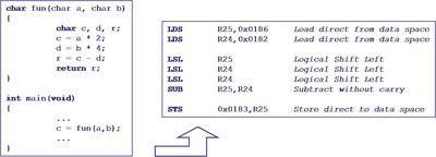
The third approach, based on an intermediate code or an assembly language, seems to be much more efficient. First of all, it allows using advanced front-end tools, existing e.g. in a GNU Compiler, to reduce the complex, high-level programming structures to simple assembler instructions. Such a process, on the simple example, is depicted in Figure 5.
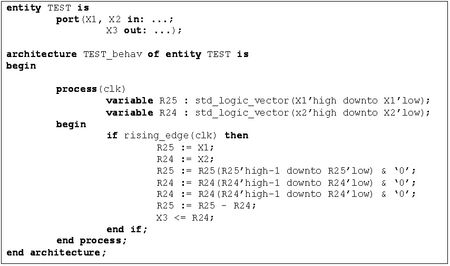
Each assembler instruction can be easily transformed into HDL description statements (Figure 6). The data dependencies as well as basic block boundaries can be extracted from the assembler code or from the compiler intermediate format (e.g. GIMPLE [5]). The compiler back-end tools can automatically generate an adequate HDL description (Figure 7).
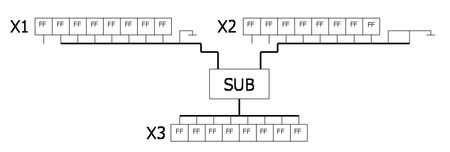
The synthesis process will generate an optimized hardware giving the functionality corresponding to the converted software operation. In this way, the results of many instructions requiring several clock cycles in the standard processor (data transfers, shifts), in the reconfigurable processor will be achieved by proper routing (Figure 8). Logic and arithmetic instructions will be performed by dedicated blocks.
Generating the operation-dedicated hardware constitutes a second source of data processing acceleration obtained in the proposed architecture.
The third source of this acceleration results from the processing parallelization. Independent logic or arithmetic instructions in the given software operation (horizontal parallelism [2]) will be implemented separately and executed concurrently, without any effort on the programmer's side.
During the hardware generating process the particular attention must be put on the length of combinational paths. Assuming a given clock synchronizing all dynamic partitions in the reconfigurable processor, the assembler to HDL converter can adapt the combinational paths to meet the clock period constraint. This can be achieved by inserting, if required, the intermediate register stages. Such structure not only allows meeting the timing requirements, but also allows implementing pipelined processing. This can be used to overlap operations from the subsequent iterations of the loop, taking the advantage of the vertical parallelism [2].
It is also possible to leave the combinational paths as they are, setting a multi-cycle constraint on them. This allows using available time more efficiently, allowing individual operations to cross clock cycle boundaries.
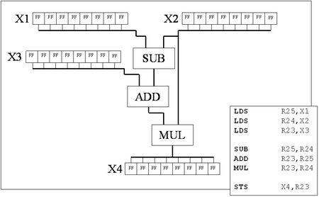
The example of such optimization can be observed for the sample operation composed of the subtraction, addition and multiplication depicted in Figure 9. Assuming that the clock cycle period is 10 ns, addition and subtraction take 6 ns each, and multiplication takes 8 ns, the asynchronous execution of the presented operation requires 20 ns – two clock cycles. When not using the multi-cycle approach, this operation has to be divided into three pipeline stages, taking 30 ns.
Reconfiguration
As mentioned above, the proposed processor cannot be efficiently implemented in commercially available reconfigurable devices. Dedicated ASIC is required. It should support high reconfiguration data transfer, with the possibility of free access to any part of the die. Reconfiguration restricted to just a row or column of existing resources, as it can be done in off-the-shelf FPGAs, increases the configuration data transfer and wastes the resources needlessly.
